- 您现在的位置:买卖IC网 > Sheet目录2000 > IDTCV142PAG (IDT, Integrated Device Technology Inc)IC FLEXPC CLK PROGR P4 56-TSSOP
COMMERCIALTEMPERATURERANGE
IDTCV142
PROGRAMMABLEFLEXPCCLOCKFORP4PROCESSOR
19
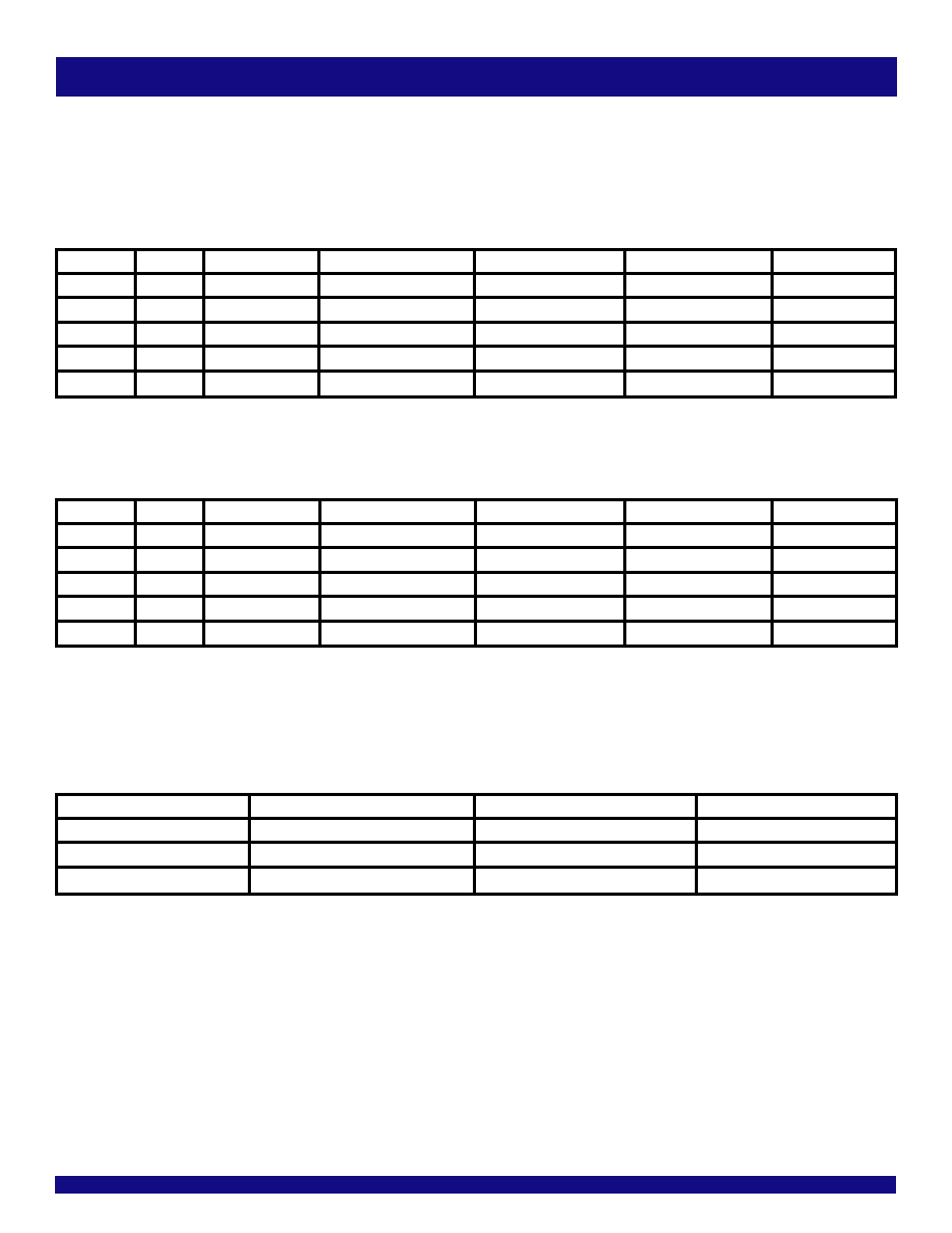
DIFFERENTIAL CLOCK TRISTATE
To minimize power consumption, CPU[2:0] clock outputs are individually configurable through SMBus to be driven or tristated during PD and CPU_STOP#
mode and the SRC clock is configurable to be driven or tristated during PCI_STOP# and PD mode. Each differential clock (SRC, CPU[2:0]) output can be
disabled by setting the corresponding output’s register OE bit to “0” (disable). Disabled outputs are to be tristated regardless of “CPU_STOP”, “SRC_STOP”
and “PD” register bit settings.
Signal
Pin PD
Pin CPU_STOP#
CPU_STOPTristate Bit
PD Tristate Bit
Non-Stoppable Outputs
Stoppable Outputs
C P U
0
1
X
Running
C P U
0
X
Running
Driven at IREF x 6
C P U
0
1
X
Running
Tristate
C P U
1
X
0
Driven at IREF x 2
C P U
1
X
1
Tristate
NOTES:
1. Each output has four corresponding control register bits; OE, PD, CPU_STOP, and “Free Running”.
2. IREF x 6 and IREF x 2 is the output current in the corresponding mode.
3. See CONTROL REGISTERS section for bit address.
Signal
Pin PD
Pin PCI_STOP#
PCI_STOPTristate Bit
PD Tristate Bit
Non-Stoppable Outputs
Stoppable Outputs
SRC
0
1
X
Running
SRC
0
X
Running
Driven at IREF x 6
SRC
0
1
X
Running
Tristate
SRC
1
X
0
Driven at IREF x 2
SRC
1
X
1
Tristate
NOTES:
1. SRC output has four corresponding control register bits; OE, PD, SRC_STOP, and “Free Running”.
2. IREF x 6 and IREF x 2 is the output current in the corresponding mode.
3. See CONTROL REGISTERS section for bit address.
Signal
Pin PD
PD Tristate Bit
Output
DOT96
0
X
Running
DOT96
1
0
Driven at IREF x 2
DOT96
1
Tristate
NOTES:
1. DOT output has two corresponding control register bits; OE and PD.
2. IREF x 6 and IREF x 2 is the output current in the corresponding mode.
3. See CONTROL REGISTERS section for bit address.
TRISTATE DOT96 CLOCK CONTROL
发布紧急采购,3分钟左右您将得到回复。
相关PDF资料
IDTCV146PVG
IC FLEXPC CLK PROGR P4 56-SSOP
IDTCV149PAG
IC FLEXPC CLK PROGR K8 56-TSSOP
IDTNW6005ASG
IC CALLER ID DECODER 20SOIC
IDTNW6006AS
IC CALLER ID DECODER 20-SOIC
IDTSSTE32882HLBBKG
IC REGISTERING CLK DRIVER 176BGA
IDTSSTE32882KA1AKG
IC REGISTERING CLK DRIVER 176BGA
ISD1750SYR
IC VOICE REC/PLAY 50SEC 28-SOIC
ISD5008EYI
IC VOICE REC/PLAY 4-8MIN 28-TSOP
相关代理商/技术参数
IDTCV142PAG8
功能描述:IC FLEXPC CLK PROGR P4 56-TSSOP RoHS:是 类别:集成电路 (IC) >> 时钟/计时 - 专用 系列:FlexPC™ 标准包装:28 系列:- 类型:时钟/频率发生器 PLL:是 主要目的:Intel CPU 服务器 输入:时钟 输出:LVCMOS 电路数:1 比率 - 输入:输出:3:22 差分 - 输入:输出:无/是 频率 - 最大:400MHz 电源电压:3.135 V ~ 3.465 V 工作温度:0°C ~ 85°C 安装类型:表面贴装 封装/外壳:64-TFSOP (0.240",6.10mm 宽) 供应商设备封装:64-TSSOP 包装:管件
IDTCV144
制造商:IDT 制造商全称:Integrated Device Technology 功能描述:PROGRAMMABLE FLEXPC CLOCK FOR P4 PROCESSOR
IDTCV145NLG
功能描述:IC CLK BUFFER 1-19 DIFF 72VFQFPN RoHS:是 类别:集成电路 (IC) >> 时钟/计时 - 专用 系列:- 标准包装:28 系列:- 类型:时钟/频率发生器 PLL:是 主要目的:Intel CPU 服务器 输入:时钟 输出:LVCMOS 电路数:1 比率 - 输入:输出:3:22 差分 - 输入:输出:无/是 频率 - 最大:400MHz 电源电压:3.135 V ~ 3.465 V 工作温度:0°C ~ 85°C 安装类型:表面贴装 封装/外壳:64-TFSOP (0.240",6.10mm 宽) 供应商设备封装:64-TSSOP 包装:管件
IDTCV145NLG8
功能描述:IC CLK BUFFER 1-19 DIFF 72VFQFPN RoHS:是 类别:集成电路 (IC) >> 时钟/计时 - 专用 系列:- 标准包装:28 系列:- 类型:时钟/频率发生器 PLL:是 主要目的:Intel CPU 服务器 输入:时钟 输出:LVCMOS 电路数:1 比率 - 输入:输出:3:22 差分 - 输入:输出:无/是 频率 - 最大:400MHz 电源电压:3.135 V ~ 3.465 V 工作温度:0°C ~ 85°C 安装类型:表面贴装 封装/外壳:64-TFSOP (0.240",6.10mm 宽) 供应商设备封装:64-TSSOP 包装:管件
IDTCV146PVG
功能描述:IC FLEXPC CLK PROGR P4 56-SSOP RoHS:是 类别:集成电路 (IC) >> 时钟/计时 - 专用 系列:FlexPC™ 标准包装:1,500 系列:- 类型:时钟缓冲器/驱动器 PLL:是 主要目的:- 输入:- 输出:- 电路数:- 比率 - 输入:输出:- 差分 - 输入:输出:- 频率 - 最大:- 电源电压:3.3V 工作温度:0°C ~ 70°C 安装类型:表面贴装 封装/外壳:28-SSOP(0.209",5.30mm 宽) 供应商设备封装:28-SSOP 包装:带卷 (TR) 其它名称:93786AFT
IDTCV146PVG8
功能描述:IC FLEXPC CLK PROGR P4 56-SSOP RoHS:是 类别:集成电路 (IC) >> 时钟/计时 - 专用 系列:FlexPC™ 标准包装:28 系列:- 类型:时钟/频率发生器 PLL:是 主要目的:Intel CPU 服务器 输入:时钟 输出:LVCMOS 电路数:1 比率 - 输入:输出:3:22 差分 - 输入:输出:无/是 频率 - 最大:400MHz 电源电压:3.135 V ~ 3.465 V 工作温度:0°C ~ 85°C 安装类型:表面贴装 封装/外壳:64-TFSOP (0.240",6.10mm 宽) 供应商设备封装:64-TSSOP 包装:管件
IDTCV149PA
功能描述:IC FLEXPC CLK PROGR K8 56-TSSOP RoHS:否 类别:集成电路 (IC) >> 时钟/计时 - 专用 系列:FlexPC™ 标准包装:1,500 系列:- 类型:时钟缓冲器/驱动器 PLL:是 主要目的:- 输入:- 输出:- 电路数:- 比率 - 输入:输出:- 差分 - 输入:输出:- 频率 - 最大:- 电源电压:3.3V 工作温度:0°C ~ 70°C 安装类型:表面贴装 封装/外壳:28-SSOP(0.209",5.30mm 宽) 供应商设备封装:28-SSOP 包装:带卷 (TR) 其它名称:93786AFT
IDTCV149PA8
功能描述:IC FLEXPC CLK PROGR K8 56-TSSOP RoHS:否 类别:集成电路 (IC) >> 时钟/计时 - 专用 系列:FlexPC™ 标准包装:1,500 系列:- 类型:时钟缓冲器/驱动器 PLL:是 主要目的:- 输入:- 输出:- 电路数:- 比率 - 输入:输出:- 差分 - 输入:输出:- 频率 - 最大:- 电源电压:3.3V 工作温度:0°C ~ 70°C 安装类型:表面贴装 封装/外壳:28-SSOP(0.209",5.30mm 宽) 供应商设备封装:28-SSOP 包装:带卷 (TR) 其它名称:93786AFT